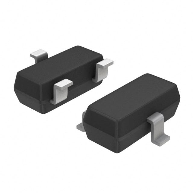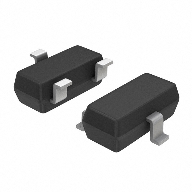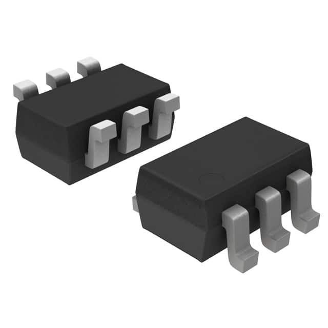
SBC857BDW1T1G ON Semiconductor TRANS 2PNP 45V 0.1A SOT-363
Дыскрэтныя паўправадніковыя прыборы
Нумар вытворцы:
SBC857BDW1T1G
Вытворца:
Катэгорыя прадукцыі:
Апісанне:
TRANS 2PNP 45V 0.1A SOT-363
Стан RoHs:
Табліцы дадзеных:
Каэфіцыент узмацнення пастаяннага току (hFE) (мінімум) @ Ic, Vce :
220 @ 2mA, 5V
Магутнасць - Макс :
380mW
Напружанне - прабой эмітэра калектара (макс.) :
45V
Насычэнне Vce (макс.) @ Ib, Ic :
650mV @ 5mA, 100mA
Пакет / Чахол :
6-TSSOP, SC-88, SOT-363
Пакет прылады пастаўшчыка :
SC-88/SC70-6/SOT-363
Працоўная тэмпература :
-55°C ~ 150°C (TJ)
серыял :
Automotive, AEC-Q101
Ток - адсечка калектара (макс.) :
15nA (ICBO)
Ток - калектар (Ic) (макс.) :
100mA
Тып мацавання :
Surface Mount
Тып транзістара :
2 PNP (Dual)
Ўпакоўка :
Tape & Reel (TR)
Частата - Пераход :
100MHz
Частка Статус :
Active
в наличии
14,586
Unit Price:
Звяжыцеся з намі Прапанова
SBC857BDW1T1G Канкурэнтныя кошты
ChipIc мае унікальную крыніцу паставак. Мы можам прапанаваць SBC857BDW1T1G больш
канкурэнтаздольную цану для нашых кліентаў. Вы можаце атрымаць асалоду ад нашым лепшым
сэрвісам, купіўшы ChipIc SBC857BDW1T1G. Калі ласка, не саромейцеся звяртацца наконт
лепшай цаны на SBC857BDW1T1G. Націсніце, каб атрымаць прапанову
SBC857BDW1T1G Асаблівасці
SBC857BDW1T1G is produced by ON Semiconductor, belongs to Транзістары - біпалярныя (BJT) - масівы.
SBC857BDW1T1G Падрабязная інфармацыя аб прадукцыі
:
SBC857BDW1T1G - гэта Транзістары - біпалярныя (BJT) - масівы, буферныя ўзмацняльнікі, распрацаваныя і
вырабленыя
ON Semiconductor.
SBC857BDW1T1G вытворчасці ON Semiconductor можна набыць на сайце Chipic.
Тут вы можаце знайсці розныя віды электронных дэталяў ад вядучых вытворцаў свету.
SBC857BDW1T1G кампаніі Chipic прайшоў строгі кантроль якасці і адпавядае усім патрабаванням.
Статус запасаў, пазначаны на Chipic, прызначаны толькі для даведкі.
Калі вы не знайшлі запчастку, якую шукаеце, вы можаце звязацца з намі для атрымання дадатковай інфармацыі, такі як колькасць запасаў у табліцы дадзеных SBC857BDW1T1G (PDF), кошт SBC857BDW1T1G, Распіноўка SBC857BDW1T1G, кіраўніцтва SBC857BDW1T1G і рашэнне на замену SBC857BDW1T1G.
SBC857BDW1T1G FAQ
:
1. What is the maximum operating temperature of the SBC857BDW1T1G?
The maximum operating temperature of the SBC857BDW1T1G is 150°C.
2. What is the typical input voltage range for this semiconductor device?
The typical input voltage range for the SBC857BDW1T1G is 0V to 40V.
3. Can you provide the thermal resistance junction-to-ambient for the SBC857BDW1T1G?
The thermal resistance junction-to-ambient for the SBC857BDW1T1G is 125°C/W.
4. What is the maximum drain current for this semiconductor component?
The maximum drain current for the SBC857BDW1T1G is 6A.
5. Does the SBC857BDW1T1G have built-in overcurrent protection?
Yes, the SBC857BDW1T1G features built-in overcurrent protection.
6. What is the typical on-state resistance of the SBC857BDW1T1G?
The typical on-state resistance of the SBC857BDW1T1G is 25mΩ.
7. Can you provide the gate threshold voltage for this semiconductor device?
The gate threshold voltage for the SBC857BDW1T1G is typically 2.5V.
8. What is the maximum power dissipation of the SBC857BDW1T1G?
The maximum power dissipation of the SBC857BDW1T1G is 2.5W.
9. Is the SBC857BDW1T1G RoHS compliant?
Yes, the SBC857BDW1T1G is RoHS compliant.
10. Can you confirm the package type and dimensions of the SBC857BDW1T1G?
The SBC857BDW1T1G comes in a DPAK package with dimensions of 6.6mm x 9.15mm.
SBC857BDW1T1G Змяненні, ключавыя словы
:
SBC857BDW1T1G Кошт
SBC857BDW1T1G Малюнак
SBC857BDW1T1G Напружанне на выснове
Акцыі: Хуткая праверка каціровак
Мінімальная замова: 1
Змяшчае прадукты серыі "SBC8"