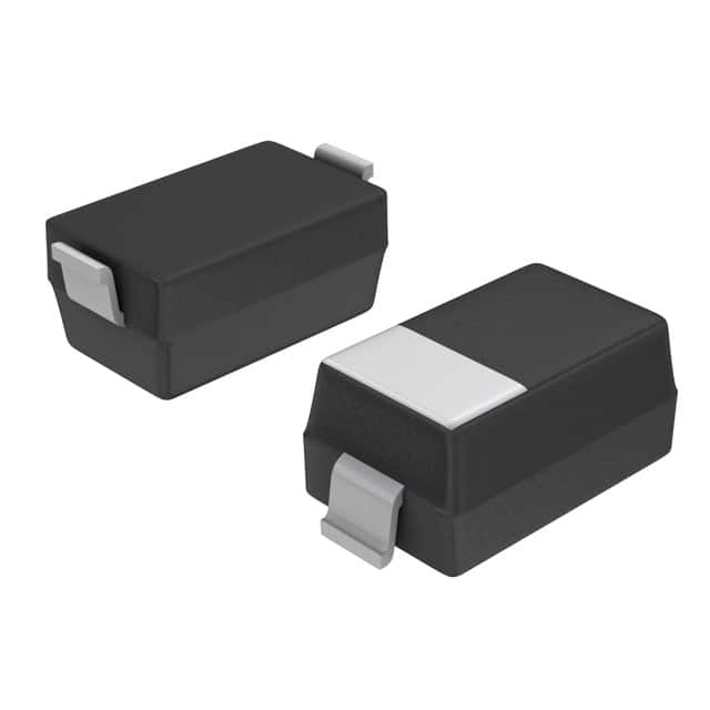
NSV45015WT1G ON Semiconductor IC REG CCR 45V 15MA SOD123
Інтэгральныя схемы (ІС)
Нумар вытворцы:
NSV45015WT1G
Вытворца:
Катэгорыя прадукцыі:
Апісанне:
IC REG CCR 45V 15MA SOD123
Стан RoHs:
Табліцы дадзеных:
Дакладнасць :
±20%
Метад зандзіравання :
High/Low-Side
Напружанне - Уваход :
45V
Пакет / Чахол :
SOD-123
Пакет прылады пастаўшчыка :
SOD-123
Працоўная тэмпература :
-55°C ~ 150°C
серыял :
Automotive, AEC-Q101
Ток - выхад :
15mA
Тып мацавання :
Surface Mount
Ўпакоўка :
Tape & Reel (TR)
Функцыя :
Current Regulator
Частка Статус :
Active
в наличии
32,879
Unit Price:
Звяжыцеся з намі Прапанова
NSV45015WT1G Канкурэнтныя кошты
ChipIc мае унікальную крыніцу паставак. Мы можам прапанаваць NSV45015WT1G больш
канкурэнтаздольную цану для нашых кліентаў. Вы можаце атрымаць асалоду ад нашым лепшым
сэрвісам, купіўшы ChipIc NSV45015WT1G. Калі ласка, не саромейцеся звяртацца наконт
лепшай цаны на NSV45015WT1G. Націсніце, каб атрымаць прапанову
NSV45015WT1G Асаблівасці
NSV45015WT1G is produced by ON Semiconductor, belongs to PMIC - Бягучы рэгуляванне / кіраванне.
NSV45015WT1G Падрабязная інфармацыя аб прадукцыі
:
NSV45015WT1G - гэта PMIC - Бягучы рэгуляванне / кіраванне, буферныя ўзмацняльнікі, распрацаваныя і
вырабленыя
ON Semiconductor.
NSV45015WT1G вытворчасці ON Semiconductor можна набыць на сайце Chipic.
Тут вы можаце знайсці розныя віды электронных дэталяў ад вядучых вытворцаў свету.
NSV45015WT1G кампаніі Chipic прайшоў строгі кантроль якасці і адпавядае усім патрабаванням.
Статус запасаў, пазначаны на Chipic, прызначаны толькі для даведкі.
Калі вы не знайшлі запчастку, якую шукаеце, вы можаце звязацца з намі для атрымання дадатковай інфармацыі, такі як колькасць запасаў у табліцы дадзеных NSV45015WT1G (PDF), кошт NSV45015WT1G, Распіноўка NSV45015WT1G, кіраўніцтва NSV45015WT1G і рашэнне на замену NSV45015WT1G.
NSV45015WT1G FAQ
:
1. What is the maximum drain-source voltage (VDS) of the NSV45015WT1G?
The maximum drain-source voltage (VDS) of the NSV45015WT1G is 150V.
2. What is the continuous drain current (ID) rating of the NSV45015WT1G?
The continuous drain current (ID) rating of the NSV45015WT1G is 45A.
3. What is the on-state resistance (RDS(on)) of the NSV45015WT1G?
The on-state resistance (RDS(on)) of the NSV45015WT1G is typically 9.5mΩ.
4. What is the gate threshold voltage (VGS(th)) of the NSV45015WT1G?
The gate threshold voltage (VGS(th)) of the NSV45015WT1G is typically 2.0V.
5. What is the total gate charge (Qg) of the NSV45015WT1G?
The total gate charge (Qg) of the NSV45015WT1G is typically 70nC.
6. What is the input capacitance (Ciss) of the NSV45015WT1G?
The input capacitance (Ciss) of the NSV45015WT1G is typically 5200pF.
7. What is the output capacitance (Coss) of the NSV45015WT1G?
The output capacitance (Coss) of the NSV45015WT1G is typically 320pF.
8. What is the reverse transfer capacitance (Crss) of the NSV45015WT1G?
The reverse transfer capacitance (Crss) of the NSV45015WT1G is typically 160pF.
9. What is the junction temperature (Tj) range for the NSV45015WT1G?
The junction temperature (Tj) range for the NSV45015WT1G is -55°C to 175°C.
10. What is the package type of the NSV45015WT1G?
The NSV45015WT1G is available in a D2PAK-3 package.
NSV45015WT1G Змяненні, ключавыя словы
:
NSV45015WT1G Кошт
NSV45015WT1G Малюнак
NSV45015WT1G Напружанне на выснове
Акцыі: Хуткая праверка каціровак
Мінімальная замова: 1
Змяшчае прадукты серыі "NSV4"