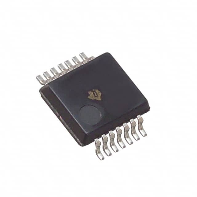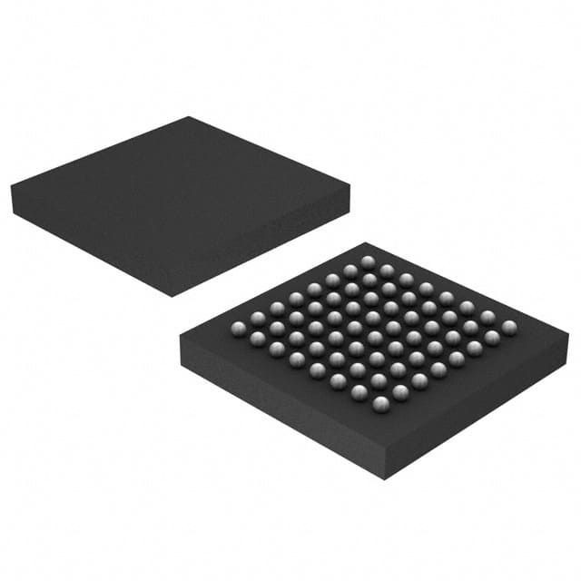
SN74LVT8986ZGV Texas Instruments IC LINK ADDRSS SCAN-PORT 64-BGA
Інтэгральныя схемы (ІС)
Нумар вытворцы:
SN74LVT8986ZGV
Вытворца:
Катэгорыя прадукцыі:
Апісанне:
IC LINK ADDRSS SCAN-PORT 64-BGA
Стан RoHs:
Табліцы дадзеных:
Колькасць біт :
-
Лагічны тып :
Linking Addressable Scan Ports
Напружанне харчавання :
2.7 V ~ 3.6 V
Пакет / Чахол :
64-LFBGA
Пакет прылады пастаўшчыка :
64-BGA MICROSTAR (8x8)
Працоўная тэмпература :
-40°C ~ 85°C
серыял :
74LVT
Тып мацавання :
Surface Mount
Ўпакоўка :
Tray
Частка Статус :
Active
в наличии
54,001
Unit Price:
Звяжыцеся з намі Прапанова
SN74LVT8986ZGV Канкурэнтныя кошты
ChipIc мае унікальную крыніцу паставак. Мы можам прапанаваць SN74LVT8986ZGV больш
канкурэнтаздольную цану для нашых кліентаў. Вы можаце атрымаць асалоду ад нашым лепшым
сэрвісам, купіўшы ChipIc SN74LVT8986ZGV. Калі ласка, не саромейцеся звяртацца наконт
лепшай цаны на SN74LVT8986ZGV. Націсніце, каб атрымаць прапанову
SN74LVT8986ZGV Асаблівасці
SN74LVT8986ZGV is produced by Texas Instruments, belongs to Логіка - спецыяльная логіка.
SN74LVT8986ZGV Падрабязная інфармацыя аб прадукцыі
:
SN74LVT8986ZGV - гэта Логіка - спецыяльная логіка, буферныя ўзмацняльнікі, распрацаваныя і
вырабленыя
Texas Instruments.
SN74LVT8986ZGV вытворчасці Texas Instruments можна набыць на сайце Chipic.
Тут вы можаце знайсці розныя віды электронных дэталяў ад вядучых вытворцаў свету.
SN74LVT8986ZGV кампаніі Chipic прайшоў строгі кантроль якасці і адпавядае усім патрабаванням.
Статус запасаў, пазначаны на Chipic, прызначаны толькі для даведкі.
Калі вы не знайшлі запчастку, якую шукаеце, вы можаце звязацца з намі для атрымання дадатковай інфармацыі, такі як колькасць запасаў у табліцы дадзеных SN74LVT8986ZGV (PDF), кошт SN74LVT8986ZGV, Распіноўка SN74LVT8986ZGV, кіраўніцтва SN74LVT8986ZGV і рашэнне на замену SN74LVT8986ZGV.
SN74LVT8986ZGV FAQ
:
1. What is the operating voltage range of the SN74LVT8986ZGV?
The operating voltage range of the SN74LVT8986ZGV is 2 V to 3.6 V.
2. What is the maximum data rate supported by the SN74LVT8986ZGV?
The SN74LVT8986ZGV supports a maximum data rate of 400 Mbps.
3. Can the SN74LVT8986ZGV be used in automotive applications?
Yes, the SN74LVT8986ZGV is qualified for automotive applications according to the AEC-Q100 standard.
4. What is the typical propagation delay of the SN74LVT8986ZGV?
The typical propagation delay of the SN74LVT8986ZGV is 2.9 ns.
5. Does the SN74LVT8986ZGV support hot insertion?
Yes, the SN74LVT8986ZGV is designed to support hot insertion.
6. What is the package type of the SN74LVT8986ZGV?
The SN74LVT8986ZGV is available in a 56-pin TSSOP package.
7. Is the SN74LVT8986ZGV RoHS compliant?
Yes, the SN74LVT8986ZGV is RoHS compliant.
8. What is the maximum quiescent current of the SN74LVT8986ZGV?
The maximum quiescent current of the SN74LVT8986ZGV is 20 mA.
9. Can the SN74LVT8986ZGV tolerate overvoltage conditions?
Yes, the SN74LVT8986ZGV has built-in ESD protection and can tolerate overvoltage conditions.
10. What is the temperature range for operation of the SN74LVT8986ZGV?
The SN74LVT8986ZGV is specified for operation over the industrial temperature range of -40°C to 85°C.
SN74LVT8986ZGV Змяненні, ключавыя словы
:
SN74LVT8986ZGV Кошт
SN74LVT8986ZGV Малюнак
SN74LVT8986ZGV Напружанне на выснове
Акцыі: Хуткая праверка каціровак
Мінімальная замова: 1
Змяшчае прадукты серыі "SN74"