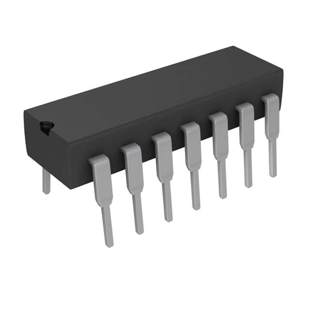
SN74LS09N Texas Instruments IC GATE AND 4CH 2-INP 14-DIP
Інтэгральныя схемы (ІС)
Нумар вытворцы:
SN74LS09N
Вытворца:
Катэгорыя прадукцыі:
Апісанне:
IC GATE AND 4CH 2-INP 14-DIP
Стан RoHs:
Табліцы дадзеных:
Асаблівасці :
Open Collector
Бягучы - у рэжыме спакою (макс.) :
-
Колькасць контураў :
4
Колькасць уваходаў :
2
Лагічны тып :
AND Gate
Макс. затрымка распаўсюджвання @ V, макс. CL :
35ns @ 5V, 15pF
Напружанне - сілкаванне :
4.75 V ~ 5.25 V
Пакет / Чахол :
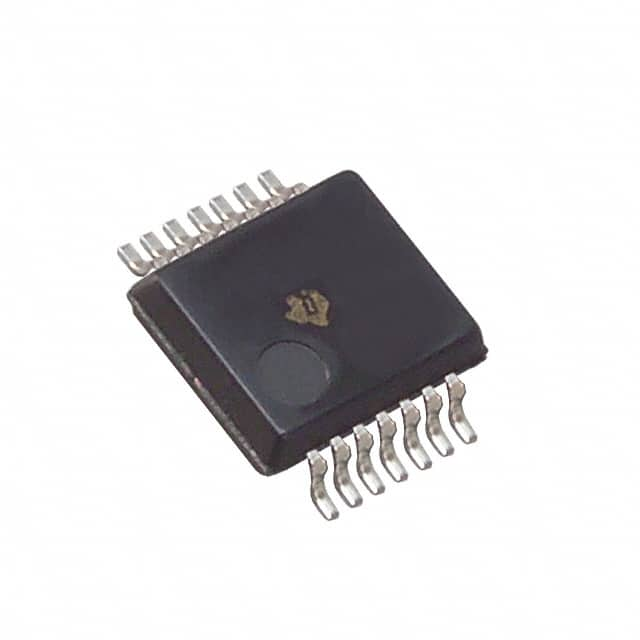
14-DIP (0.300", 7.62mm)
Пакет прылады пастаўшчыка :
14-PDIP
Працоўная тэмпература :
0°C ~ 70°C
серыял :
74LS
Ток - выхад высокі, нізкі :
-, 8mA
Тып мацавання :
Through Hole
Узровень логікі - высокі :
2V
Узровень логікі - нізкі :
0.8V
Ўпакоўка :
Tube
Частка Статус :
Active
в наличии
35,369
Unit Price:
Звяжыцеся з намі Прапанова
SN74LS09N Канкурэнтныя кошты
ChipIc мае унікальную крыніцу паставак. Мы можам прапанаваць SN74LS09N больш
канкурэнтаздольную цану для нашых кліентаў. Вы можаце атрымаць асалоду ад нашым лепшым
сэрвісам, купіўшы ChipIc SN74LS09N. Калі ласка, не саромейцеся звяртацца наконт
лепшай цаны на SN74LS09N. Націсніце, каб атрымаць прапанову
SN74LS09N Асаблівасці
SN74LS09N is produced by Texas Instruments, belongs to Логіка - вароты і інвертары.
SN74LS09N Падрабязная інфармацыя аб прадукцыі
:
SN74LS09N - гэта Логіка - вароты і інвертары, буферныя ўзмацняльнікі, распрацаваныя і
вырабленыя
Texas Instruments.
SN74LS09N вытворчасці Texas Instruments можна набыць на сайце Chipic.
Тут вы можаце знайсці розныя віды электронных дэталяў ад вядучых вытворцаў свету.
SN74LS09N кампаніі Chipic прайшоў строгі кантроль якасці і адпавядае усім патрабаванням.
Статус запасаў, пазначаны на Chipic, прызначаны толькі для даведкі.
Калі вы не знайшлі запчастку, якую шукаеце, вы можаце звязацца з намі для атрымання дадатковай інфармацыі, такі як колькасць запасаў у табліцы дадзеных SN74LS09N (PDF), кошт SN74LS09N, Распіноўка SN74LS09N, кіраўніцтва SN74LS09N і рашэнне на замену SN74LS09N.
SN74LS09N FAQ
:
1. What is the function of the SN74LS09N integrated circuit?
The SN74LS09N is a quad 2-input positive AND gates IC, which means it contains four separate AND gates that each have two inputs and one output.
2. What is the operating voltage range for the SN74LS09N?
The operating voltage range for the SN74LS09N is typically between 4.75V and 5.25V.
3. What is the maximum input current for the SN74LS09N?
The maximum input current for the SN74LS09N is 1μA.
4. What is the maximum output current for the SN74LS09N?
The maximum output current for the SN74LS09N is 8mA.
5. What is the maximum propagation delay for the SN74LS09N?
The maximum propagation delay for the SN74LS09N is 15ns.
6. What is the power dissipation of the SN74LS09N at 25°C?
The power dissipation of the SN74LS09N at 25°C is typically 10mW.
7. What is the operating temperature range for the SN74LS09N?
The operating temperature range for the SN74LS09N is between 0°C and 70°C.
8. What is the pin configuration of the SN74LS09N?
The pin configuration of the SN74LS09N is as follows: Pin 1 - Input A1, Pin 2 - Input B1, Pin 3 - Output Y1, Pin 4 - Input A2, Pin 5 - Input B2, Pin 6 - Output Y2, Pin 7 - GND, Pin 8 - VCC.
9. What is the package type of the SN74LS09N?
The SN74LS09N is available in a 14-pin DIP (Dual In-line Package).
10. What are some common applications for the SN74LS09N?
The SN74LS09N is commonly used in digital logic design, arithmetic circuits, and general-purpose switching applications.
SN74LS09N Змяненні, ключавыя словы
:
SN74LS09N Кошт
SN74LS09N Малюнак
SN74LS09N Напружанне на выснове
Акцыі: Хуткая праверка каціровак
Мінімальная замова: 1
Змяшчае прадукты серыі "SN74"